IC & Sensor Packaging Technology 2018 will be between 17 Jan and 19 Jan 2018.
The location of the Exhibition will be Tokyo Big Sight which is one of the fantastic venue for such an essential event.
IC & Sensor Packaging Technology 2018 may be a medium where many highly recommended products and solutions are exhibited. Several of these tend to be about Packaging Technology, Packaging Materials, Packaging, Packaging Components and Manufacturing.
19th Exhibition for IC Final Manufacturing gathering Advanced Equipment, Materials and Services is an annual Exhibition.
The organizer of the IC & Sensor Packaging Technology 2018, 19th Exhibition for IC Final Manufacturing gathering Advanced Equipment, Materials and Services is Reed Exhibitions Japan Ltd..
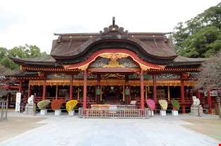
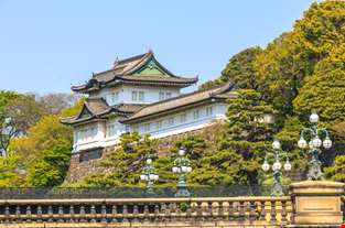
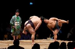
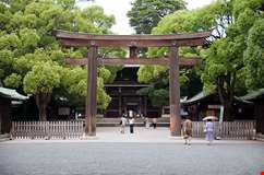
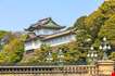
When you are in Tokyo for IC & Sensor Packaging Technology 2018, explore these three must visit places and fall in love with the charm of this city:
Held inside NEPCON JAPAN.
Visitor Profile
- Semiconductor Manufacturers
- Assembly Manufacturers/SATS
- Sensor Manufacturers
- Set Manufacturers (in high-density SMT)
- MEMS Devices/LED Manufacturers
- Automotive Electronics Manufacturers
Exhibitor Profile
- Assembly Equipment
- Packaging Materials/Components
- Analysis/Simulation Software for IC Packaging
- Various Packages

Venue
Tokyo Big Sight
Address : 3 Chome-11-1 Ariake, Kōtō-ku, Tōkyō-to 135-0063, Japan
Travel Guide
Concurrent Events

17 - 19 January 2018

17 - 19 January 2018

10th International Exhibition for LED / OLED Technology and Application 2018
Tokyo, Japan
17 - 19 January 2018

35th Exhibition on Test, Inspection, Measurement and Analysis for Electronics Manufacturing and R&D 2018
Tokyo, Japan
17 - 19 January 2018
Other Events in Tokyo


12 - 14 June 2024
load time : 63ms
- last update time : 28-02-2017
Event Type
Organizer
Reed Exhibitions Japan Ltd.
Official Site
Weather of Tokyo

17 °C
Clear clear sky
Report Error


Leave Your Comment